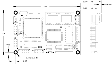
Connectors
J1 General I/O & Synchronous Serial
J2RS-485
J3COM1
J4COM2 (Console)
J5Multi-I/O Bus (General I/O)
J8Power
J10 Ethernet
JP1 Watchdog NMI Enable
JP2 Socket Memory Type
JP3 Boot Memory Location
Specifications
ProcessorIntel 386Ex, 25MHz
Operating System XDOS(MS/PC DOS 3.3 compatible)
Memory 512K SRAM, 512K Flash
Ethernet 10BASE-T, NE2000 compatible
Serial Port 1 RS-232 with 5 handshake lines
Serial Port 2 RS-232 no handshaking or
Digital I/O 10 Bits: P3.0-P3.5 & P1.4-P1.7,
Watchdog Programmable Timeout,
Sync. Serial Full duplex
Independent Rx and Tx clocks,
Supply Voltage 5V DC ±5%
Supply Current 400mA(nominal)
Humidity 5 - 90%, non-condensing
Temperature -20 to +85 °C
Weight 1.6oz (45 gm)
Dimensions 3.75" x 2.50" x 0.63"
(95mm x 63.5mm x 16mm)
I/O Port DC Characteristics
Symbol Parameter MIN MAX Units Condition
VIL Input Low -0.3 0.8 V
VIH Input High 2.0 Vcc+0.3 V
VOL Output Low 0.45 V IOL= 8mA
VOH Output High Vcc-0.5 V IOH= -8mA
Mating Connectors
Connector Mfg MFG P/N JK micro P/N
J1,J3,J4,J5 (2x5) Molex 22-55-2101
Pins (for 2x5) Molex 16-02-0096
J2,J8 (1x3) Molex 22-01-2031
J10 (1x8) Molex 22-01-2081
Pins (for 1x3, 1x8) Molex 08-50-0114
Optional Features
M-Systems DiskOnChip Flash Disk, 512K SRAM, 512K Flash, or Battery backed clock calendar chip with 128K SRAM (20-0074)
Multi-I/O or µI/O peripheral boards for I/O expansion.
uFlash TCP Technical Information
12228 E Bennett Rd. Grass Valley, CA 95945
Phone (530) 297-6073
Fax (530) 297-6074
© 2016 JK microsystems, Inc. All rights reserved.

Offering embedded computer solutions since 1996